Replace silicon with new materials is reshaping the landscape of computing, inviting researchers and industry players to rethink what makes a modern processor tick, from core device physics to software stacks and data-center cooling strategies, and it sets the tone for a new era of design and collaboration. As performance and energy efficiency become top priorities, researchers are exploring silicon replacement materials and a spectrum of approaches that could extend Moore’s law without relying solely on shrinking features, including improved device architectures, novel deposition techniques, and better defect control in pilot fabs, this long-term effort reshaping investment priorities, talent pipelines, and standards across the supply chain. The first wave includes wide-bandgap semiconductors, 2D materials, and engineered oxides, each promising higher voltages, better thermal performance, and reduced leakage, alongside efforts in alternative materials for chips, which aim to unlock efficient power management, faster switching, and resilience in harsh environments. Industry eyes are on the convergence of materials science and manufacturing innovations in semiconductors, where the challenge is not only discovering a new substance but integrating it into existing fabs and supply chains, a path toward next-gen semiconductor materials that preserves yield, minimizes cost, and leverages retooling rather than wholesale replacement, with regulatory alignment to ensure safe, scalable adoption. In this context, semiconductor materials research is expanding beyond silicon toward layered ecosystems that empower data centers, AI accelerators, and edge devices while preserving cost and reliability, with collaborative programs spanning universities, startups, and chipmakers aimed at clear, testable milestones, including independent benchmarks and real-world pilots.
Beyond silicon, industries are exploring alternative substrates, exotic compounds, and new device paradigms that could power the next wave of computing across mobile, cloud, and edge workloads. Candidate families range from wide-bandgap semiconductors and 2D materials to complex oxides and perovskites, all evaluated for how they could improve energy efficiency, thermal management, and data movement in future chips. The emphasis is on CMOS-friendly integration, scalable growth methods, and reliable performance across billions of devices, not just dramatic laboratory demonstrations. As collaboration between academia, startups, and major manufacturers deepens, the industry is building a multi-layered adoption path that preserves the silicon ecosystem while expanding options for high-end logic, memory, and interconnects.
Landscape of silicon replacement materials and why it matters
The race to replace silicon isn’t about a single blockbuster switch but a portfolio of approaches that blend several material families to extend performance and efficiency beyond traditional scaling. At center stage are silicon replacement materials and next-gen semiconductor materials that aim to reduce heat, leakage, and power draw while delivering higher performance per watt.
In practice, the current landscape spans wide-bandgap semiconductors, 2D materials, and engineered alloys. Each class brings distinct advantages—and distinct integration hurdles—making this a multi-front, synergetic effort rather than a single silver bullet. The success of these efforts also hinges on manufacturing innovations in semiconductors that bridge lab breakthroughs to high-volume production.
Wide-bandgap pioneers: GaN, SiC, and Ga2O3 shaping power and RF
Wide-bandgap semiconductors such as GaN, SiC, and Ga2O3 offer higher breakdown voltages and superior efficiency for power electronics and RF applications. These materials can dramatically reduce energy loss and enable higher switching speeds, which is essential for data centers, electric vehicles, and telecom infrastructure.
While GaN and SiC are established in niche power devices, expanding their use to logic and mixed-signal roles requires continued process development, wafer-scale growth control, and reliable integration with existing fabrication lines. This is a central pillar of the broader semiconductor materials research aimed at sustainable performance improvements in the era of alternative materials for chips.
Replace silicon with new materials: A roadmap for next-gen semiconductor materials
A gradual, multi-stage adoption path is expected rather than an overnight replacement. Near-term milestones focus on specialized applications such as high-efficiency power devices and RF components, with mid-term efforts expanding CMOS compatibility and standardized testing procedures. This roadmap reflects a broader program of semiconductor materials research and a measured approach to integrating new materials into production.
The strategy emphasizes hybrid architectures, modular manufacturing enhancements, and cross-cutting reliability studies. For alternate materials for chips, the journey includes qualification, packaging integration, and cost-of-ownership analyses that balance performance gains with the realities of price pressure and toolchain disruption.
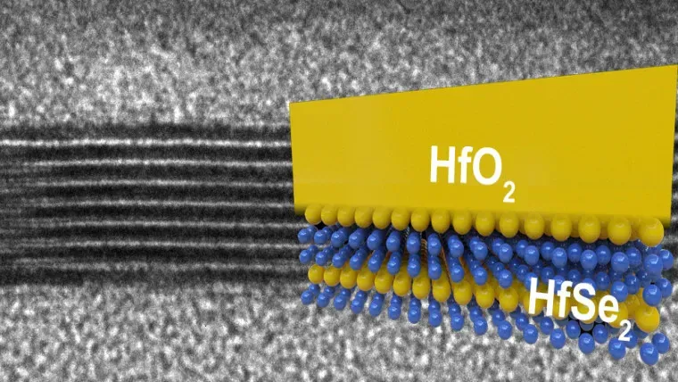
Two-dimensional materials for high-speed logic and interconnects
Graphene and transition metal dichalcogenides such as MoS2 and WS2 offer exceptional electron mobility and atomically thin channels that, in theory, could yield faster transistors with lower parasitic capacitance. These properties position 2D materials as appealing candidates for niche logic, ultra-fast interconnects, and specialized sensors.
In practice, achieving large-area, defect-free synthesis and stable transistor behavior at scale remains a major hurdle. The path to widespread adoption depends on breakthroughs in wafer-scale growth, defect control, and process integration within CMOS workflows—a core focus of ongoing semiconductor materials research.
Oxides, perovskites, and novel memory for logic and neuromorphic computing
Complex oxides and perovskite materials bring potential for new memory architectures, neuromorphic computing, and optoelectronic integration that could complement silicon’s capabilities. While photovoltaics have driven much of perovskite research, continued exploration targets logic and memory functions that could reshape future devices.
Integration challenges include stability, reproducibility, and compatibility with CMOS process flows. Ongoing semiconductor materials research is evaluating deposition methods, interface engineering, and packaging strategies that could unlock reliable, scalable implementations in future systems.
Industry landscape: collaboration, manufacturing innovations in semiconductors, and adoption timelines
The push to replace silicon with new materials is a collaborative multi-player sport, involving universities, national labs, startups, and major semiconductor companies. A three-pronged strategy—targeted, application-specific deployments; hybrid approaches within CMOS; and long-horizon exploratory research—animates this ecosystem.
Adoption timelines suggest near-term wins in power electronics and RF, with broader CMOS integration developing gradually. The overall success depends on manufacturing innovations in semiconductors, scalable deposition or growth methods, and sustained semiconductor materials research that translates lab breakthroughs into reliable, cost-effective products.
Frequently Asked Questions
Why is Replace silicon with new materials considered necessary, and what are the leading silicon replacement materials being explored?
Replacing silicon is driven by fundamental scaling limits such as heat dissipation, leakage, and rising lithography costs. The leading silicon replacement materials include wide-bandgap semiconductors like GaN, SiC, and Ga2O3 for power and RF, as well as 2D materials such as graphene and MoS2, and engineered alloys like Ge/SiGe and oxide or perovskite systems. Each material offers unique advantages but also integration challenges, which is why this remains a multi-front effort rather than a single silver bullet.
What role do next-gen semiconductor materials play in the race to Replace silicon with new materials?
Next-gen semiconductor materials are pursued for higher performance per watt, faster data movement, and better thermal management across computing, data centers, and mobile devices. They cover a spectrum from power electronics to high-speed logic and interconnects, with materials such as GaN, SiC, 2D compounds, and oxide-based systems. Realizing these gains requires solving fabrication, reliability, and integration challenges on mainstream rails.
How do manufacturing innovations in semiconductors impact the viability of Replace silicon with new materials at scale?
Manufacturing innovations in semiconductors—wafer-scale synthesis, CMOS compatibility, and new deposition and etching chemistries—are the gatekeepers for scale. Achieving consistent quality, low defect density, and acceptable total cost of ownership determines whether a promising material can move from lab to production. Without robust, repeatable processes, even strong performance advantages may not translate into affordable devices.
What opportunities do alternative materials for chips open for future devices?
Alternative materials for chips open opportunities in high-efficiency power devices, RF components, specialized sensors, and potentially neuromorphic or memory-centric architectures. These materials can deliver performance or energy benefits in targeted applications, paving the way for a layered ecosystem alongside silicon. The challenge is to validate reliability and cost in real products.
What does semiconductor materials research tell us about the timeline for broader adoption of Replace silicon with new materials?
Semiconductor materials research suggests a gradual transition rather than a rapid replacement. Near-term milestones (2-5 years) focus on specialized apps with clear ROI, mid-term (5-10+ years) on broader CMOS integration, and long-term prospects for new computing paradigms built on multiple silicon-free or silicon-lean technologies.
How might the industry realize a layered ecosystem where silicon remains dominant while new materials contribute?
The most likely path is a layered ecosystem in which silicon handles mass-market logic while silicon replacement materials power high-performance, energy-efficient, and specialized devices. Hybrid approaches and co-design enable stepwise gains, supported by collaboration across academia, startups, and incumbents to reduce risk and shorten time-to-market.
| Aspect | Key Points | Notes / Details |
|---|---|---|
| Silicon’s Role & Limits | Silicon powers the digital era; limits include heat dissipation, leakage, and the rising cost of advanced lithography; performance per watt is increasingly critical. | A primary driver for exploring new materials; not a single technology shift, but a spectrum of approaches. |
| What ‘New Materials’ Mean | Diverse candidates across classes such as wide-bandgap semiconductors, 2D materials, and engineered compounds. | Approaches complement silicon and address different parts of the performance puzzle. |
| Wide-Bandgap Candidates | GaN, SiC, Ga2O3 offer higher breakdown voltages and improved efficiency for power electronics and RF. | GaN/SiC are established in power devices; broader CMOS logic integration is an active area of development. |
| 2D Materials | Graphene and MoS2, WS2 provide exceptional mobility and ultra-thin profiles for fast devices. | Challenges include large-area, defect-free synthesis and stable transistor behavior at scale. |
| Ge & SiGe Channels | Ge or SiGe channels and strained silicon/heterostructures boost mobility within CMOS. | Integration within existing fabrication lines remains a key pathway to higher performance. |
| Perovskites & Oxides | Complex oxides and certain perovskites could enable novel logic, memory, neuromorphic, or optoelectronic functions. | Most work to date centers on photovoltaics; expanding to logic/memory is an active area. |
| Diamond & Thermal Management | Diamond and related materials offer superior thermal conductivity for heat removal in high-performance devices. | Useful for telecom, power modules, and HPC to manage heat; not the primary semiconducting channel. |
| Integration & Manufacturing Realities | Wafer-scale growth, defect control, and CMOS compatibility are critical hurdles. | Total cost of ownership and reliability are major considerations for adoption. |
| Industry Landscape & Collaboration | A three-pronged strategy: targeted deployments, CMOS-hybrid integration, and long-horizon exploratory research. | Collaboration among universities, national labs, startups, and large semiconductor companies accelerates progress. |
| Roadmap to Adoption | Near-term focus on high-efficiency power devices and niche sensing; mid-term broader CMOS integration; long-term new computing paradigms. | Adoption will be gradual and layered, not an overnight replacement. |
| Impact & Takeaways | For consumers: faster, cooler devices; for businesses: energy efficiency gains and new product opportunities. | Policy support and sustained investment in materials science are important to accelerate progress. |
Summary
Replace silicon with new materials is driving a multi-front race that could redefine the backbone of computing. As industry explores Replace silicon with new materials, the focus is on integrating wide-bandgap semiconductors, 2D materials, and oxide compounds with CMOS processes to achieve higher performance per watt. Near-term wins will come from targeted deployments in power electronics and high-speed interconnects, while mid- and long-term efforts aim to extend Moore’s law through scalable manufacturing and reliable integration. The result could be a layered ecosystem: silicon for mass-market logic, complemented by new materials for high-performance, energy-efficient devices across data centers, mobile, and specialized sensing. Realizing this vision requires sustained investment in materials science, scalable deposition techniques, defect management, and cross-disciplinary collaboration to translate lab breakthroughs into manufacturable products. For consumers, the payoff is faster, cooler, and more efficient devices; for businesses, new capabilities, differentiated offerings, and improved total cost of ownership. In short, the race to Replace silicon with new materials is a strategic expansion of the toolkit guiding the next wave of computing resilience and capability.